Inspecting a PCB
With Easy3D, it is possible to use depth maps for PCB inspection. This section presents a simple detection of missing or misplaced components on a PCB. The processing is done entirely with 2D images but use depth maps as inputs.
The workflow is as follow:
Perform a 3D acquisition or create the depth map with software laser line extraction (
ELaserLineExtractor.NET Python class). Retrieve the grayscale image corresponding to the depth map (EDepthMap8::AsEImage.NET Python method).Align the image using fiducial markers (
EMatcher.NET Python class).Search for the PCB plane and subtract it from the aligned image, only the components and the connectors remain (
EasyImage::Oper.NET Python function with parameterEArithmeticLogicOperation_Subtract.NET Python).Compare the processed image to a golden sample to detect missing or misplaced components (
EasyImage::Oper.NET Python with parameterEArithmeticLogicOperation_Compare.NET Python orEChecker.NET Python).
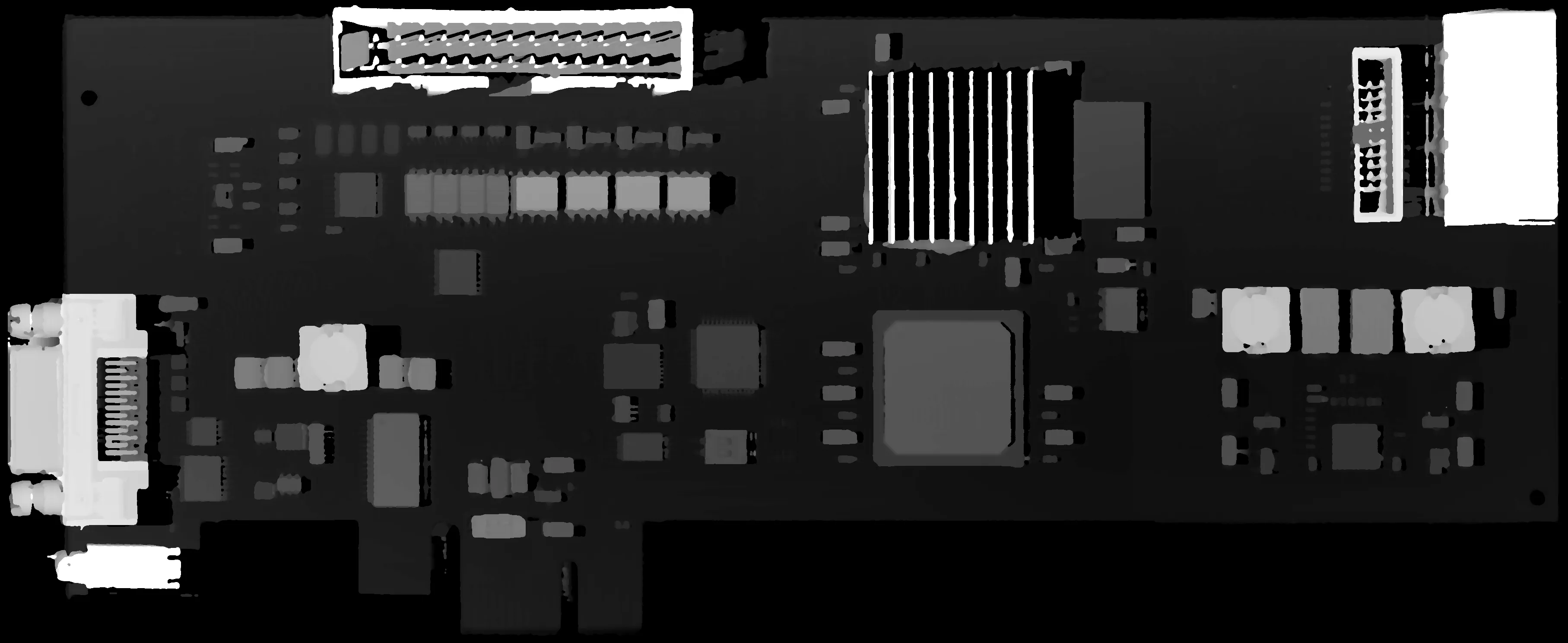
The source depth map of a PCB, outputs of CoaxLink Quad 3D-LLE
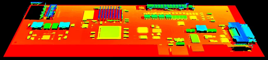
The same depth map displayed as a 3D point cloud with false colors
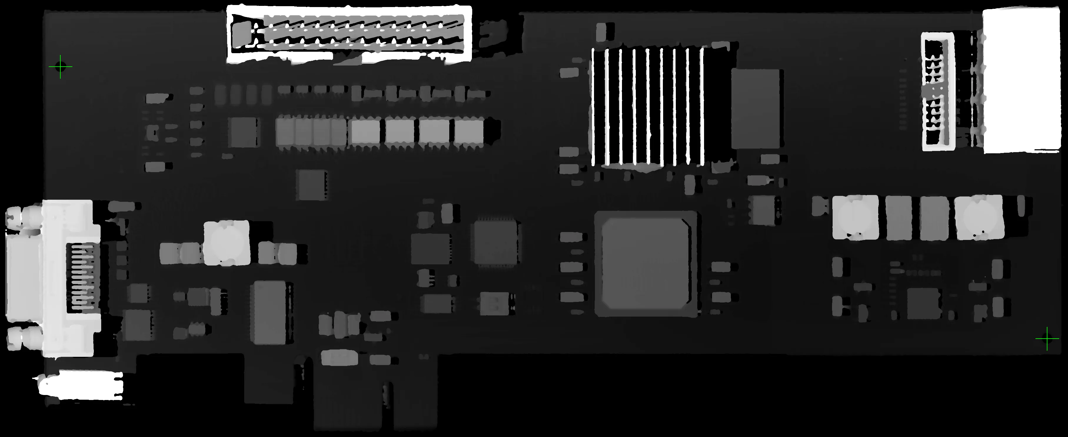
Align the image using fiducial markers (2 holes)
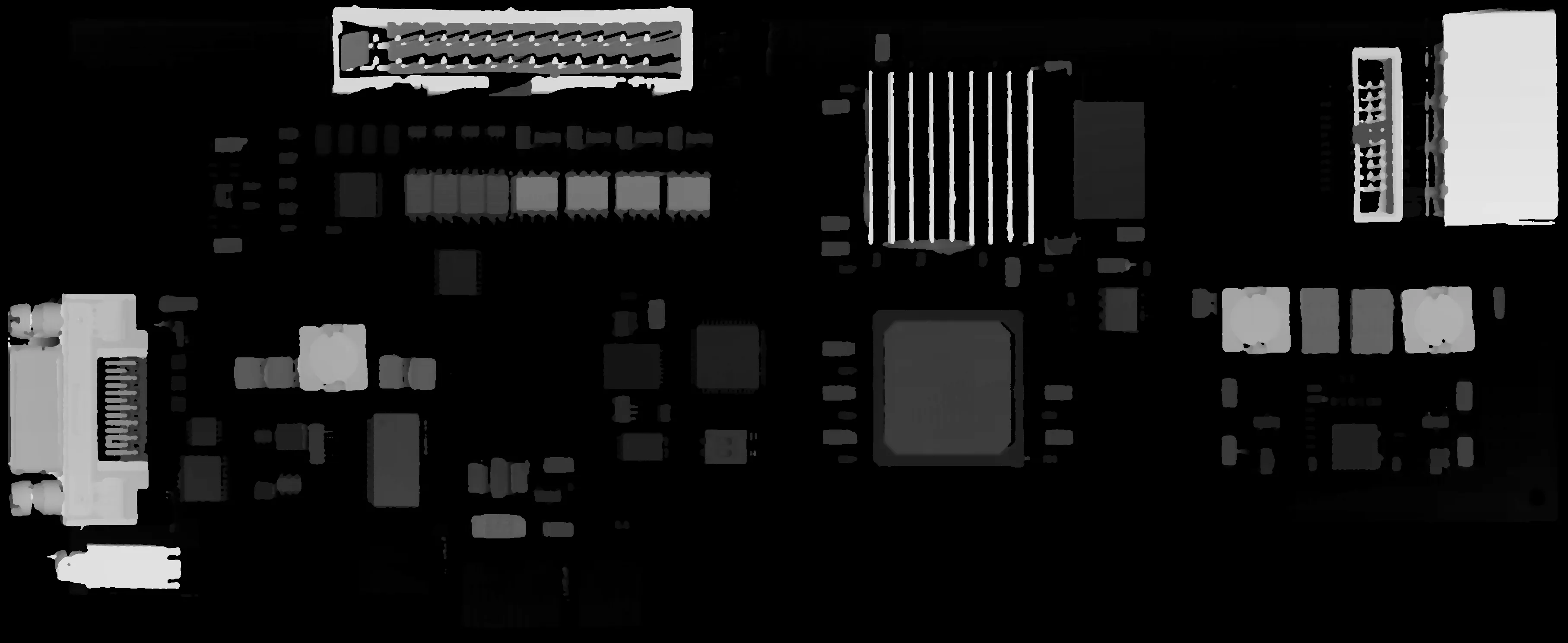
The image with reference plane subtracted, leaving only the components
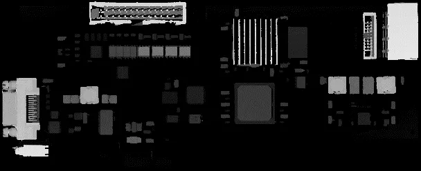
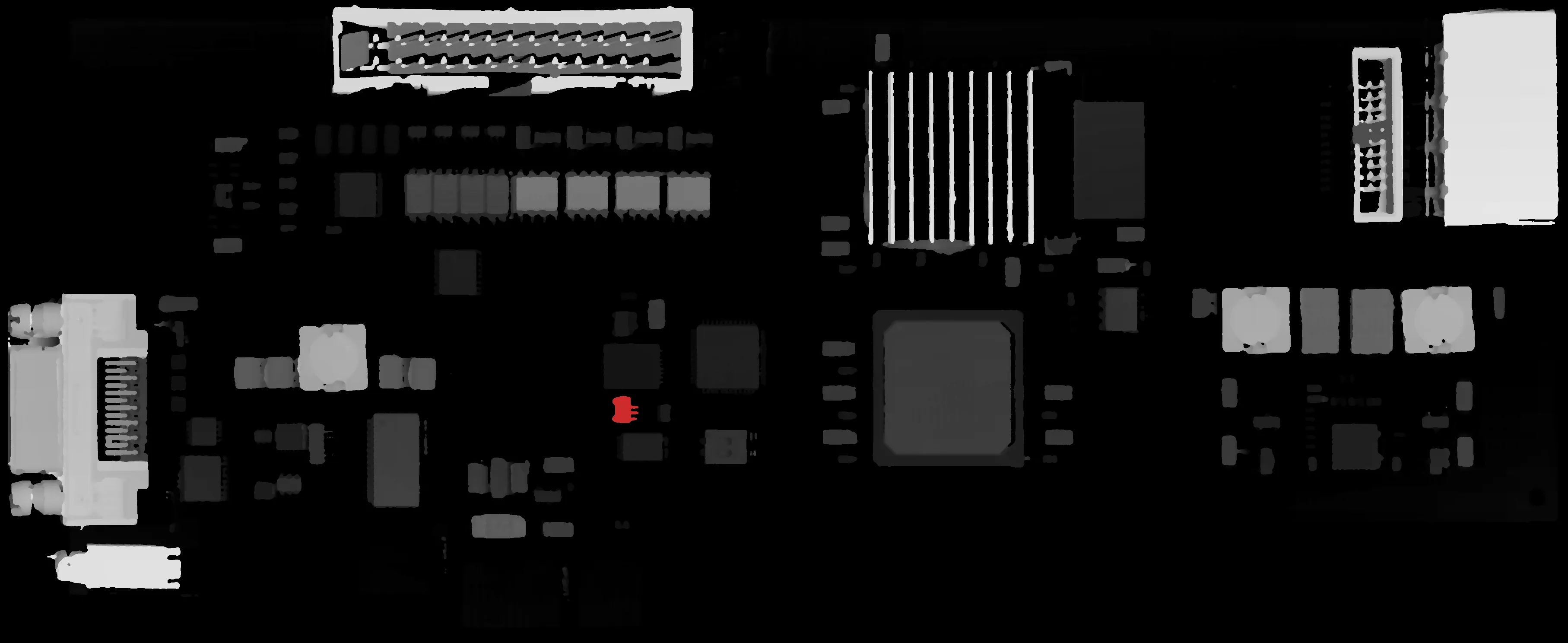
The comparison of the image (left) with the golden sample (right, processed with the same workflow) shows the missing component (in red)